
search
MANUFACTURING CAPABILITIES SUMMARY
Capability
CEM-3,FR-4(Normal to High Tg),High CTI FR-4,Polyimide(PI) ,Aluminum Base,Rogers
HAL, HASL Leadfree, ENIG, Chem Tin, OSP, Gold Finger, Immersion Silver, ENEPIG
4mil/0.1mm
1080, 2116, 7628, 106, 3313, 2165, 1500.
24.41X47.24inch/620X1200mm
Min. base copper 1/3Oz
Max. base copper 10Oz
2- Layer 0.2mm/8mil
4-Layer 0.35mm/14mil
6-layer 0.65mm/26mil
8-Layer 1.0mm/40mil
10-Layer 1.3mm/51mil
12-Layer 1.6mm/63mil
14-Layer 1.8mm/71mil
16-Layer 2.0mm/79mil
Max.table size: 685X685mm
Max.inspect size: 620X620mm
Max. thickness: 3.20mm(126mil)
Min. thickness: 0.10mm(4mil)-core
Min. width/gap: 3mil/3mil
3mil track width, 3mil tracks width/gap, IPC class 2/IPC class 3,Flying probe/tooling test, Differential impedance, TDR testing, Automatic optical inspection
±0.10mm(4/6layers)
±0.13mm(8/10layers)
±0.15mm(12/14/16layers)
6.0mm/236mil
3/3mil
4mil/0.1mm
≧25µm
12:01
±0.075mm/3mil(Standard), ±0.05mm/2mil(Advanced)
±0.05mm/2mil (On laminate area)
±0.03mm (On ground area)
±0.075 (Standard) ±0.05mm (Advanced)
±0.13 (2nd drilled hole to 1st drilled hole location (mm)
±0.075mm (board thickness≤1.0mm)
±0.10mm (board thickness>1.00mm)
±0.10mm (Standard), ±0.076mm (Advanced)
≥8mil (0.2mm)
>1012Ω
<300Ω
10A
1.4N/mm
>6H
288℃ 20Sec
>20-300V
>4mil/0.1mm
>(50Ω-100Ω) ± 10% (Standard)、(50Ω-100Ω) ± 7% (Advanced)
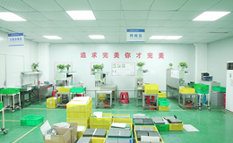
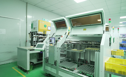
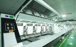
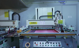
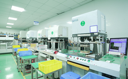
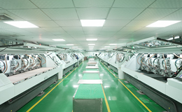
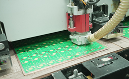
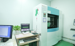
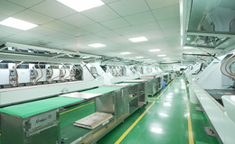
MANUFACTURING EQUIPMENTS AT KESHIJIA
For more than 14 years, we have been produced printed circuit boards for over 2500 companies throughout Europe, North America and Asia, including factories and distributors.Our manufacturing facilities dose inspect the whole materials and manage the whole production process carefully to ensure quality control.
Product Category

COMPANY
LET'S STAY IN TOUCH