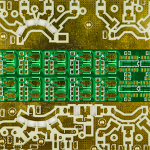
PCB Blind Buried Via & HDI PCB

Blind Via:

A blind via is a copper plated hole that is interconnected to only one external layer of the PCB. However, it is important to know that the hole does not go all the way to the board, making it “blind” or “invisible” to the naked eye.


Buried Via:

A buried via connects at least two layers without going to the outer edges of the board. So it is buried within the circuit and completely internal.
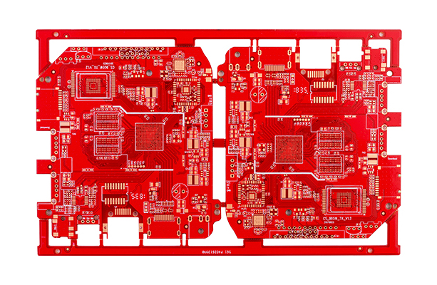
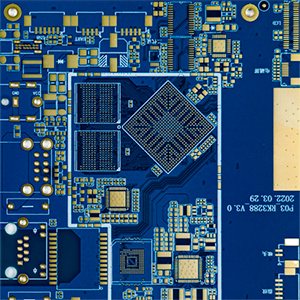
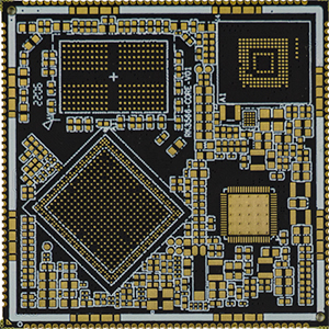
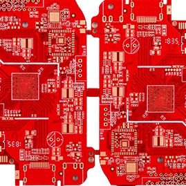
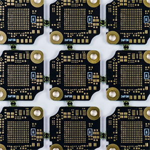

HDI PCBs:

HDI as a printed circuit board with a higher wiring density per unit area than conventional printed circuit boards (PCB).

product structure

Using micro blind holes to increase the line distribution density, improve radio frequency and electromagnetic wave interference, heat conduction. Application in servers, mobile phones, digital cameras, etc.

KSJ Circuits PCB Certifications & Registrations

While your repeat business best illustrates our commitment to excellence, we also hold advanced PCB certifications to verify our extremely rigorous standards.

MANUFACTURING EQUIPMENTS AT KESHIJIA

For more than 14 years, we have been produced printed circuit boards for over 2500 companies throughout Europe, North America and Asia, including factories and distributors.Our manufacturing facilities dose inspect the whole materials and manage the whole production process carefully to ensure quality control.

View All Equipment

GET IN TOUCH

We'd love to hear from you!