Via in Pad Fr4 PCB

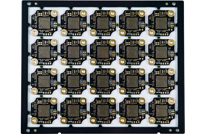
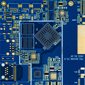
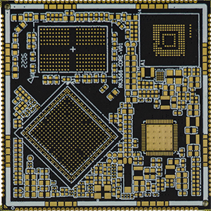
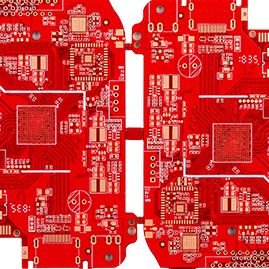
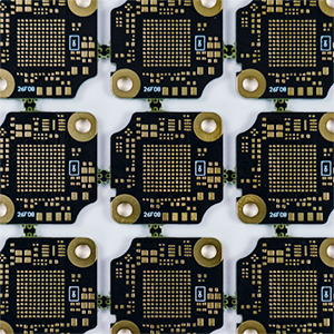
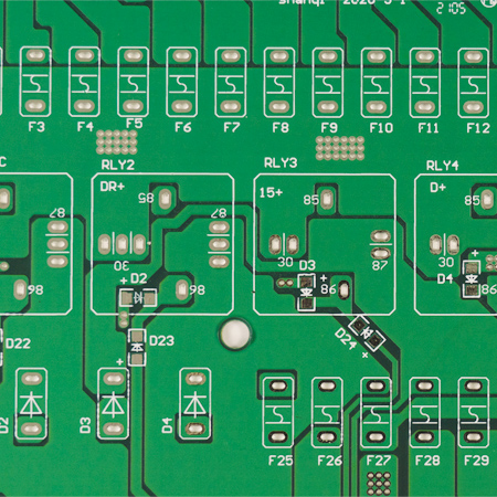
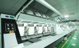
Via-in-pad (VIP) technology is the technology by which via is placed directly beneath component contact pad, especially BGA pad with finer pitch array packages. In other words, VIP technology leads to vias plated or hidden under BGA pad, requiring PCB manufacturer should plug via with resin prior to carrying out copper plating on the via to make it invisible.

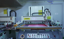
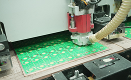
Using electroplating to fill holes/resin plug holes, to prevent solder paste or flux from flowing into  holes in the pad, prevent solder beads or ink pads in the holes from causing false soldering.

product structure

• Fit for fine pitch BGAs; • Leading to higher density of PCBs ,saving space; • Performing better in thermal management, beneficial for heat dissipation; • Defeating constraints of high-speed designs such as low inductance; • Sharing a flat surface with component attachment; • Making PCB footprints smaller and routing further and better; • Application in the Bluetooth module of the consumer electronics industry, etc.

KSJ Circuits PCB Certifications & Registrations

While your repeat business best illustrates our commitment to excellence, we also hold advanced PCB certifications to verify our extremely rigorous standards.

MANUFACTURING EQUIPMENTS AT KESHIJIA

For more than 14 years, we have been produced printed circuit boards for over 2500 companies throughout Europe, North America and Asia, including factories and distributors.Our manufacturing facilities dose inspect the whole materials and manage the whole production process carefully to ensure quality control.

View All Equipment

GET IN TOUCH

We'd love to hear from you!