
search
ELECTRICAL TEST
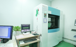
Bare Printed Circuit Board Electrical Testing Capabilities
Keshijia, as a regular part of its PCB manufacturing process, performs electrical testing on your printed circuit boards to ensure their quality. Below please find a full explanation of how we perform these tests and what they mean. As a leading PCB manufacturer we assure you that we monitor for quality here in our own facilities, where we fabricate your printed circuit boards; we are not a broker. Your PCB order is manufactured by us and tested by us so you will know that your printed circuit boards are free of defects and meet the standards you expect.
We currently have two different types of testing equipment available to test your circuit boards; we have a number of Everett Charles ATG test machines that are flying probe, fixtureless testers and we also have universal grid testing capability. These machines use fixtures built specifically for your PCB.
Bare Board Testing
Bare board testing involves using capacitance and resistance tests; each of our machines uses a combination of both. Capacitance testing for a bare board involves testing for opens and shorts by "charging" a net or plane and then probing each net to measure the induced capacity. Inaccuracies occur with this method because of the inherent variability in producing circuit boards. However field measurement or field effect testing for shorts uses a very similar approach.
Resistance Testing
Resistance testing measures the resistance found in the net. As electric current flows through a conductor collisions between electrons and atoms interfere with the flow of the electrons. This is known as resistance and it's measured in ohms.
A good conductor has LOW resistance - at common temperatures silver is the best conductor and copper is second. The amount of resistance depends on the conductor's length and its cross-sectional area. If you have two circuits of the same material and the same cross-section and one is twice as long as the other - the longer one has TWICE as much resistance. If you have two circuits of the same material and the same length but one is twice as thick as the other - the thicker conductor will have HALF the resistance.
So Resistance is proportional to length and inversely proportional to the cross-sectional area of a conductor and dissipates power in the form of heat.
Using CAD/CAM Data
KSJ PCB' test processes use CAD/CAM data for ALL test programs and optimize both ATG and Trace test programs while meeting Class 2 requirements. We follow the IPC 9252 specification guidelines for Class 2 testing processes, which means that we test 100% of the networks on the board for continuity and isolation (that's opens and shorts) using a test program generated from your Gerber data. We do not test 100% of the points - we optimize out mid points of nets as allowed by the standard. We do not use your original Gerber data - it does not guarantee a 100% test.
Electrical Test Terminology
• 100% Net List Test: Check of every "node" on every net on the board.
• Adjacency Test: Type of test for checking isolation between conductors - shorts test. A software generated program that checks for nets that are within a tolerance set by the user.
Two methods are used - Proximity Adjacency and Line of Site Adjacency.
• Clam Shell Test: Provides simultaneous testing of both sides of the board at the same time. These types of fixtures are used on single grid testers and dual grid testers. A very reliable
method of bare board testing because all points are tested at the same time.
• Combined Grid/Probe Testing: Using the flying probe test sequence to cover areas of the board with fine pitch, high density points while the grid test verifies power to ground
separation, through hole and wider pitch component pads.
• Comparative or Golden Board Test: Method using a "master" or known good board (KGB) to learn a program and then test other boards against the learned net list program. Poor
choice for test accuracy - you may be learning a "bad" board.
• Continuity Test: Verification that the resistance between test points is lower than the specified limit or maximum continuity resistance. See shorts and opens tests.
• End of Net: A feature which is either the origin or the termination of a conductor network.
• Endpoint: A test point or node required to be tested to meet the 100% continuity and isolation test.
• Field Effect and Field Measurement Test: Refer to a type of test that uses large nets as antennas to send a specific high frequency alternating current at a specific voltage. The
remaining nets are checked and those that have similar voltages for all antennas are considered as shorted and then retested using Ohm's law resistance to verify the shorts.
• Flip Test: Consists of two separate, independent single sided tests on a universal grid. Testing one side and then the other. Unless a significant number of points are tested during both
tests it can be a very inaccurate method.
• High Pot Test: Refers to high voltage potential testing to check for high resistance continuity or leakage between ground and power planes. DC voltages in the 500 to 1000 volt ranges
are used for a specified dwell time.
• Impedance: The design of a circuit and the frequency of the current passing through it have various affects on the alternating current passing through it. The combination of these
effects and the resistance of the conductor is called impedance.
• Impedance Control Test: A device called a TDR (Time Domain Reflectometer) is used to check circuits to determine if they are within expected tolerances. Conductor length, spacing,
width, height and separation affect the impedance.
• In Circuit Test: Test performed after components are installed - a check for shorts or opens caused during assembly operations.
• Isolated Land:A test point not connected to any other test point or net. Also called a single point net, singlet or no connect.
• Isolation Resistance: The resistance tolerance between the circuit board's non-connected traces and/or lands.
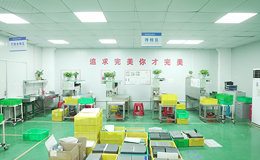
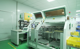
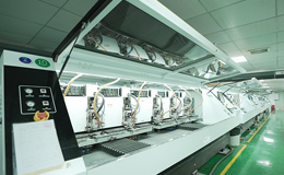
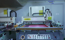
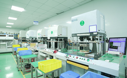
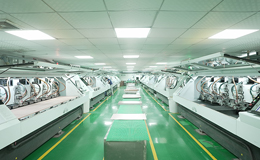
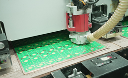
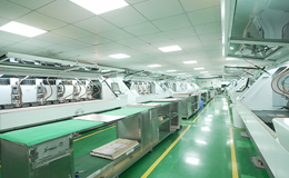
MANUFACTURING EQUIPMENTS AT KESHIJIA
For more than 14 years, we have been produced printed circuit boards for over 2500 companies throughout Europe, North America and Asia, including factories and distributors.Our manufacturing facilities dose inspect the whole materials and manage the whole production process carefully to ensure quality control.
Product Category

COMPANY
LET'S STAY IN TOUCH